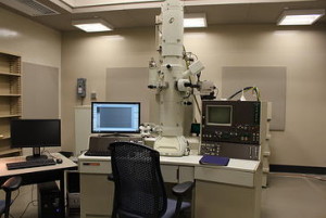
JEOL 2011 High-Resolution TEM
The JEOL JEM- 2011 scanning TEM equipped with a bottom-mounted Gatan SC1000 CCD camera and an EDAX EDS system is a multipurpose high-resolution analytical electron microscope with a wide range of capabilities:
- Bright-field and dark field imaging
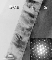
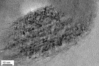
- High-resolution imaging
- Selected-area electron diffraction (SAED), nano-beam and convergent-beam electron diffraction
- Micro-area x-ray analysis for compositional analysis
TEM provides internal microstructure information of materials including:
- Crystallographic structure
- Grain and grain boundary structures in bulk, polycrystalline and nanostructured materials
- Dislocations, stacking faults, twins domain and domain boundaries, precipitates and particles
- Interfaces down to the atomic level
TEM operating specifications:
- Accelerating Voltage: 80-200kV
- Magnification (steps): 50-1,500,000
- Specimen Tilt Angle: ±35°
- Lattice Resolution: 0.14nm
- Point Resolution: 0.23nm